Wednesday, December 19, 2007

Development Board - Microcontroller 8051

AES Development Kit

Microcontroller 8051

(P89C/V51RD2 & AT89S52)

Contents:

1. AES 8051-DK (Complete PCB mounted with basic circuitry)

2. 16x2 LCD module.

3. A.C Adaptor (6 volts)

4. Serial Cable.

5. Programmer cable for AT89S52

6. Connectors for ports. (4 for 4 ports and 1 for ULN)


Overview of the Kit

The development kit AES 8051-DK is a versatile kit designed to implement all the possible projects to be build around microcontroller 8051. The kits is also provided with basic on board interfaces such as ULN driver which can be used to drive light loads as LED’s as well as heavy loads like stepper motor.


Advanced Embedded Solutions : Development Kit for 8051 Microcontroller. Image 1

Interfaces provided on board for R&D purpose.

1. ULN2803 on port 0: 8 LED’s are connected to the output of the driver. LED’s should be enabled by placed a jumper on the 2 pin connector placed besides LED’s. A connector is also provided at the output of ULN. Other loads (ex. Stepper motor) can be connected at this connector. If driving load other then LED’s, remove the jumper.

2. Input Switches: 8 push-button switches are provided at port 1. These switches can be used as basic input device.

3. 16x2 LCD module: The LCD module is connected on board. Data bus of LCD is connected to port 2 (D0-D7). To enable LCD place a jumper on the two pin connector located below the LCD module. Control signals of LCD are derived from port 3 as mentioned in the above list.

4. Serial Communication: A MAX-232 transceiver is provided on board with capacitors (voltage doubling circuit), which provides serial communication between the Development board and serial port of P.C. This circuit is also used to program the microcontroller through serial port. The circuit should be enabled by placing two jumpers on the connectors (RXD, TXD), prior to use.

5. Besides the basic peripherals mentioned above each port is connected to a 10 pin connector (8 port pins & Power i.e. Vcc, Gnd), for the user to interface some other device if required.

Advanced Embedded Solutions : Development Kit for 8051 Microcontroller. Image 2

Powering up the AES 8051-DK

· The kits can be supplied by both A.C and D.C (one at a time), depending on the supply available with the user.

· The adaptor provided with the kit is a 6volt (A.C, 750mA) adaptor which can be directly plugged into the round shaped connector on board labeled as AC. Rectifier circuit is on board.

· The user can also provide a D.C supply of 12 volts to adjacent connector labeled as 12VDC.

· In both the cases the voltage to microcontroller circuit is provided through 7805 regulator IC.

· A push-button lock switch (labeled as AC/DC) provided selection between A.C & D.C supply (if one connects both).

· Pushing the switch to down position selects A.C supply. Releasing the switch selects D.C supply.


Installing the AES 8051-DK

1. Connect the A.C adaptor output to the connector on PCB.

2. Connect the serial cable provided with the kit on DB-9 connector (labeled as RS-232) between the Kit and the serial port of P.C.

3. Place jumpers on the pins (TXD, RXD).

4. Power up the system by pressing the push-button switch.(AC/DC)

5. The kit is ready for programming.


A tutorial on Philips flash magic:

Programming the microcontroller P89C/V51RD2BN using Philips Flash Magic

1. Open the Philips flash magic software.

2. Make the following setting in the software:

· Select the appropriate COM port where the kit is connected.

· Select the Baud rate (Generally keep it at 9600)

· Select the device (89C51RD2xx or 89V51RD2) according to the microcontroller place on board.

· Place a tick on “Erase all flash”

3. Brows your code’s .HEX File I the hex file space.

4. Click on the “Start” button.

5. The software gives a message “Reset the device in ISP mode now” (in case of 89V51RD2)

6. Turn the kit off by pressing the pushbutton switch (AC/DC) switch and then switch it on. The above box disappears and the hex file gets transferred.

ALTERNATIVELY

6. At this point press the “BOOT” switch on the kit. Reset the device by pressing the “RESET” switch (while keeping the BOOT switch pressed), and then release the BOOT switch. The above window disappears and the .HEX file is transferred to the microcontroller.

7. After the software shows “Finish” (bottom right of the window) Press “RESET” switch to execute your program.

8. In case of 89C51RD2xx, select this device, locate the hex file, follow STEP 6 (above) and then press start button on the software.

A tutorial on RIDE:

Executing sample programs using RIDE.

1. Open the RIDE software.

2. To make a new project:

Project ---------> New

· Specify a “Name”.

· Directory where the project is to be stored.

· Target family as 80C51.

· Click “Next”.

· Select the target device as: Atmel-AT89S52, or Philips-P89C/V51RD2xx.

· Clock on “Finish”

3. The place on the left hand side is the project window. It shows all the details about the project.

4. To create new file: File New C File.

5. Write your code into the window on the right and save it.

6. Right click on your project name in the project window and click on “Add node source/application”.

7. Brows the saved C-File and click ok. This includes the C-File in the project.

8. To generate .HEX file of the project press F9. The hex file is generated is there are no errors in the code.

9. The location of the .HEX file is shown at the bottom of the RIDE window.

10. This file can be directly transferred to the microcontroller using Flash magic.


Friday, June 29, 2007

APPLICATION SPECIFIC INDUSTRIAL ROBOT

ASIR: APPLICATION SPECIFIC INDUSTRIAL ROBOT

STRUCTURE:::
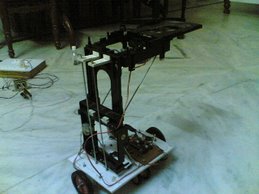
This is basically a special pick and place mechanism. It is a prototype for any industrial transport operations. The machine in the picture below is a robot made out of CD tray. The mechanism of the CD tray has been directly used for the job. As seen one CD tray provides movement along one co-ordinate axes. So two trays are used to provide movement along two co-ordinate axes. One tray is placed on vertically and the other is place on this tray horizontally. So a combination of these two trays provide motion along two co-ordinate axes. This complete assembly is place on a four a vehicle which is a four wheel drive. The vehicle consists of four geared motors each having a torque of 2 Kgs. Each CD tray has a single motor that pushes or pulls the tray out or in respectively. The vertical tray holds the horizontal tray. So when the vertical tray gets a signal it is pulled up and hence the horizontal tray in closed position moves upward with it.
So the trays provide motion along two co-ordinate axes and the vehicle can move in the horizontal plane so combining the horizontal plane motion and the movement of the tray in upward direction we have motion along three co-ordinate axes. The motion along the co-ordinate axes can be controlled by the microprocessor based control system described below.


Image 1 Both trays open

Image 2

CIRCUIT:::

The machine is completely autonomous and doesn't require any command externally. It is completely microprocessor controller system. Micro-controller 89C51RD2BN is used as the central processor of the machine. The motor drivers are L293D (Dual H-Bridge). The total number of motors in the machine are six. Four are used to drive the vehicle and the other two are used for the movement of the tray. All these six motors can be rotated in forward or reverse direction by giving appropriate signals to the drivers (L293D).


Image 3 Both trays closed

Image 4.

Watch Video:


Tuesday, June 26, 2007

Design of Execution Unit for 8-bit Processor & Implementation in VHDL

BLOCK DIAGRAM

Description of Block Diagram:


The above block diagram shows the complete design of the processor. It consists of an 8-bit ALU which is used to perform all the arithmetic and logical instructions. Four 8-bit general purpose working registers namely A (Accumulator) and registers B, C and D are used to store the results. The program status word (PSW) presently consists of two flags: Carry flag and Zero flag. Only these two flags are needed according to the current design of the processor. The PSW can be expanded later on to include Parity flag, Auxiliary flag and others when designing new instructions. The instructions to the processor are fed through the instruction register which is a 16-bit register via the 16 bit input bus to the processor. The main function of the instruction decoder is to separate the different fields from the 16-bit number received from the instruction register .The instruction decoder decodes the instructions and provides the required data to each of the blocks. It generates the required control signals to execute a particular instruction and provides the data accordingly to the registers and the ALU.

The design consists of four 8-bit general purpose input/output ports namely A, B, C and D. Each port consists of a port register which is used to send data to the port or receive data from the port. The blocks are connected via the system buses. A 16 bit input bus to the system provides the instruction and the data to the processor. Timing and control unit generates the required control signals for execution of instructions.


INSTRUCTION EXECUTION AND INSTRUCTION DECODER FORMAT:

As stated in the abstract earlier that the design does not conists of the bus interface unit which is generally required for fetching the instructions and data from the external memory. The instruction are provided using a DIP switch and executed when switch pb1 is pressed. So, in this section we describe what happens when this switch is pressed. The instruction register is provided with the instruction as soon as the switch is pressed. The instruction register passes o this instruction to the instruction decoder. The instruction decoder the separates the fields from the 16-bit number provided to it. It then provides the different blocks with different data fron this 16-bit number. Let us consider an example at this place. Suppose the instruction fed to the processor is

ADD A,#22H. Which is add immediate data 22(Hex) to the Accumulator register and store the result in Accumulator itself. The format of instruction decode is as shown below. The bits 15 to 13 indicate the opcode that is the instruction. Bit 12 indicates the addressing mode. Addressing mode refers to the style in which the data is provided to the processor. Bits 11-8 indicate the destination. And bit 7-0 indicates the source of the data. Thus as the instruction is put into the instruction decoder the fields are separated and the processor know what operation is to be performed, what is the addressing mode, what is the destination of the result(port or register) and what is the source of the data. In our example (the add instruction) the addressing mode is immediate so the data is present in the instruction and is the last 8 bits (LSB) of the instruction. Also the destination is Accumulator. It should also be noted that the operation is to be performed on Accumulator so one of the data is present in the Accumulator to which the immediate data is to be added. Now the processor clearly knows what it has to do to get the results. As ADD is an arithmetic instruction the processor needs to use ALU for executing this instruction. Before we analyze the flow of the instruction let us summarize the complete information provided to the processor by the instruction.


Bits 15-13 => Instruction <=


Bit 12 =>’1’ Addressing Mode =>Immediate


Bits 11-8 => Destination <= Accumulator


Bits 7-0 => Data (As addressing mode is immediate)


Bits

15-13

Bit

12

Bits

11-8

Bits

7-0


OPCODE ADDRESSING DESTINATION SOURCE

MODE


VHDL Code


The simulation results obtained by Simulating the Code on ModelSim 6.3 are shown below:

FIG.1 Instruction Register


FIG.2 ALU

FIG.3 Synchro. Unit

Sunday, June 24, 2007

MICROMOUSE: An Autonomous Robot

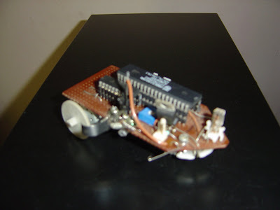
Electronic circuitry : Details regarding sensors, microcontroller, motor driver. Microcontroller P89C51RD2BN is the heart of the circuit. The sensing is done via GP2D12 (Distance Sensing module by SHARP). The analog output voltage of the sensor is given to ADC 0804. The ADC is interfaced to Microcontroller unit. 5 volt D.C motors (Coil resistance: 12 ohm) are the thrusters to the mouse driven by L293D (Driver). The microcontroller provides appropriate control signals to the motors through driver after sensing the input from the sensors. Simple limit switch is used for the front wall detection. The supply to the circuit is provided through 9 volt rechargeable battery using 7805 regulator.

The microcontroller is programmed using serial port of the computer. The clocking circuitry for the Microcontroller and the ADC is provided separately on the same PCB.

Image 1

Mouse Structure : Details regarding chassis, positioning of sensors, wheels . The mouse structure is made totally out of scrap. The complete mouse structure has the maximum dimension as: Length = 11 cm, Breadth = 7 cm and Height = 5 cm.

The main PCB itself acts as the mouse structure. Two motors are tied beneath this PCB at the back (clearly visible in the bottom view above). Gears of diameter 2.6 cm are fixed to the motor shaft, which acts as the wheels of the mouse. A ball roller mechanism (made out of scrap) is attached below the PCB in front to provide free wheeling action. Both the sensors (side and front) are attached to the PCB and remain stationary throughout.

The structure of the mouse is clear from the IMAGE 2 below.

Image 2

The two specialty of the mouse are as follows:

1. The mouse structure is made out of scrap. The motors are pulled out from an old CD ROM. The wheels (Gears) are also from the scrap CD ROM mechanism. The ball roller mechanism (provided for free wheeling action in the front) is also made using part of an old floppy drive. The front wall sensor is a simple limit switch taken from an old mechanism.

2. The second specialty of this mouse is the size: The mouse can easily fit into a box with dimensions:

11 x 7.5 x 5 (All dimensions in cm). The size of the mouse can also be depicted from the IMAGE 1. As seen from this image the mouse can easily fit in the palm of my hand. For efficient utilization of the circuit space on the PCB the space below the IC’s is also utilized for placing the circuit components.

Thus the cost of the mouse is only the cost incurred in the circuit components.


Image 3